Reprogramming "old" Sennheiser SKM 3072-U - Part 2 - I2C
Understanding what is going on I2C
write to 0x3E ack data: 0xE0 0xC8 0xF0 0x00 0x00 0x00 0x00 0x00 0x00 0x00 0x00 0x00write to 0x3E ack data: 0xE0 0x00 0x00 0x00 0x00 0x00 0x00 0x00 0x00 0x00 0x00 0x00write to 0x50 ack data: 0x10read to 0x50 ack data: 0x11write to 0x51 ack data: 0x1Aread to 0x50 ack data: 0xA9write to 0x51 ack data: 0xB3read to 0x50 ack data: 0x1Fwrite to 0x51 ack data: 0xAEread to 0x50 ack data: 0x03write to 0x51 ack data: 0xAFread to 0x50 ack data: 0x20write to 0x51 ack data: 0xACread to 0x50 ack data: 0xFCwrite to 0x51 ack data: 0xADread to 0x50 ack data: 0x5Dwrite to 0x51 ack data: 0xC4read to 0x50 ack data: 0xFCwrite to 0x51 ack data: 0xC5read to 0x50 ack data: 0x41write to 0x50 ack data: 0x14read to 0x50 ack data: 0x00write to 0x50 ack data: 0x11read to 0x50 ack data: 0x03write to 0x51 ack data: 0x1Dread to 0x50 ack data: 0xBBwrite to 0x51 ack data: 0x1Eread to 0x50 ack data: 0x99write to 0x51 ack data: 0x1Fread to 0x50 ack data: 0x8Cwrite to 0x51 ack data: 0x73read to 0x50 ack data: 0x78write to 0x51 ack data: 0x74read to 0x50 ack data: 0x26write to 0x51 ack data: 0x75read to 0x50 ack data: 0xFEwrite to 0x7F ack data: 0x5D 0x06 0x83 0xF00x370xEF0x88 0x5E 0x260xFC0xE1 0x6Fwrite to 0x3E ack data: 0xE0 0x00 0x00 0x00 0x00 0x00 0x9F 0x00 0x00 0x00 0x00 0x00write to 0x3E ack data: 0xE0 0x00 0xF0 0x00 0x00 0x00 0xFB 0x00 0x00 0x00 0x00 0x90write to 0x3E ack data: 0xE0 0x00 0xBF 0x00 0x09 0x00 0x9A 0x00 0x00 0x00 0x00 0xF0write to 0x3E ack data: 0xE0 0x00 0xAB 0x00 0x0F 0x00 0xBD 0x0F 0x00 0x00 0x00 0x99write to 0x3E ack data: 0xE0 0x00 0xDA 0x00 0x09 0x00 0x00 0x9B 0xF0 0x00 0x00 0xBFwrite to 0x3E ack data: 0xE0 0x00 0x0D 0x00 0x9B 0x00 0x7B 0xFA 0xBF 0x00 0x00 0x09write to 0x3E ack data: 0xE0 0x00 0xF0 0x00 0x00 0x00 0xEF 0x0B 0x00 0x00 0x00 0x2Fwrite to 0x50 ack data: 0x11 0x03write to 0x50 ack data: 0xB1read to 0x50 ack data: 0x11write to 0x50 ack data: 0x73read to 0x50 ack data: 0x79write to 0x50 ack data: 0x74read to 0x50 ack data: 0x87write to 0x50 ack data: 0x75read to 0x50 ack data: 0x00write to 0x50 ack data: 0xB1read to 0x50 ack data: 0x11write to 0x3E ack data: 0xE0 0x00 0xBA 0xFF 0x99 0x00 0xFB 0xDF 0xFA 0xF7 0xBF 0xFFwrite to 0x50 ack data: 0x73read to 0x50 ack data: 0x79write to 0x50 ack data: 0x74read to 0x50 ack data: 0x87write to 0x50 ack data: 0x75read to 0x50 ack data: 0x00write to 0x50 ack data: 0xB1read to 0x50 ack data: 0x11write to 0x3E ack data: 0xE0 0x00 0xBA 0xFF 0x99 0x00 0xFB 0xDF 0xFA 0xF7 0xBF 0xFFwrite to 0x7F ack data: 0x41 0xF00x37write to 0x3E ack data: 0xE0 0x00 0x37 0xFF 0xE3 0x00 0x75 0x61 0x1C 0xF7 0xBF 0x26write to 0x50 ack data: 0x73read to 0x50 ack data: 0x79write to 0x50 ack data: 0x74read to 0x50 ack data: 0x87write to 0x50 ack data: 0x75read to 0x50 ack data: 0x00write to 0x50 ack data: 0xB1read to 0x50 ack data: 0x11write to 0x3E ack data: 0xE0 0x00 0xBA 0xFF 0x99 0x00 0xFB 0xDF 0xFA 0xF7 0xBF 0xFF
Just like this is not very helpful. But I already know there are 3 devices on the bus. EEPROM, PLL and LCD driver. By little bit of playing around I have found out that 0x3E is display since it I can see it changing in the log as I'm pushing the buttons. It even makes lot of sense since you can see quite huge portions of data sent to the address the display has 6 times 8 segment for displaying numbers, 2 dots, 2 times bar graph for audio and RF 8 segments each, RF labels and BAT label. That means 6*8+2+2*8+2= 68 segments. So I would need around 9 bytes to encode it all, naively speaking. So it actually makes sense. And datasheet for it is nowhere to find and since I don't have to care anyway its enough.
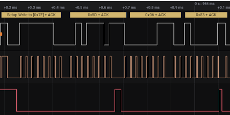
There is also mysterious 0x7F which I suspected to be PLL. After looking at the manual I have found out that it need to set on of its inputs LOW in order to accept the data from I2C. So I added next channel to logic analyzer which was hooked to this pin. And started recording.
Then there is 0x50 and 0x51. This actually confused me a lot on the beginning but after all it can be simply put into the phrase RTFM (Read The F* Manual) well, in this case EEPROM datasheet. It truly is EEPROM as suspected and its address is described in the DS. You can change the address by setting high or low two of its inputs. So in theory you may create array of 4 EEPROM using same chip. But in the mic both E1 and E2 are set low, so the address should be 0x50. Then why 0x51? As clear from the table below, the memory is split into two blocks(halves) and by setting last bit of its address you can choose the block!
write to 0x51 ack data: 0x1Aread to 0x50 ack data: 0xA9
Parsed it means: Device 0x50 read data from block 1 of address 0x1A, and response with the data 0xA9.
But in which format are the data stored in the EEPROM and how can they be safely modified?


Komentáře
Okomentovat